This article has been published 90 days after I contacted Renesas PSIRT. They were nice and just asked me to wait. This vulnerability is listed as CVE-2021-43327.
It all started with this device I had on my table with a Renesas RX65 inside. I wanted to read its code and reverse it.
As I never worked with Renesas devices, I didn't have any clue on how to proceed. After a bit of research, I understood there was no support for this chip in OpenOCD or any other open source tool so I would have to use the proprietary tools.
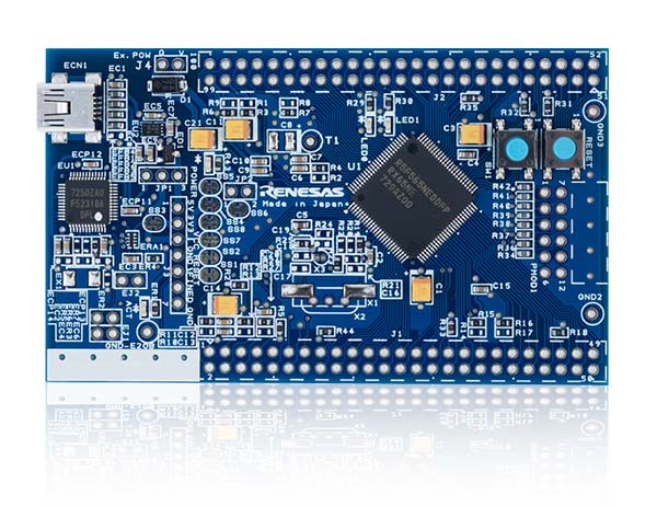
I first looked for an evaluation board for this chip. Luckily enough there is an affordable Renesas Target board with this chip family. The Renesas Target Board for RX65N (RTK5RX65N0C00000BR):
It has an integrated on-chip debugger (E2-Lite) so we can read and write flash with the Renesas Flash Programmer GUI.
Having this evaluation board, I decided to solder my "to be read" chip on it. No problem so far. However, when I tried to read the flash memory content, I discovered the chip was protected and I needed a 16 bytes ID code....
In order to (hopefully) find a way to read this flash, I first needed a way to interact with the device without using the GUI.
The RX family can be started in Boot Mode. After release from reset state, depending on the MD and UB pins configuration, the booloader is activated in one of these modes:
FINE is a proprietary interface used by Renesas and is not documented. USB is also not documented, so the easiest option is to use the serial interface.
The serial protocol is well documented and it has commands to erase, read and write flash.
This is what the documentations explain:
"The flash memory supports various security functions. The security function includes protection of ID codes for the serial programmer, protection of ID codes for the on-chip debugger, disabling the connection of serial programmer, and protection of the ROM codes.
In serial programming, protection of ID codes for serial programmer and prohibiting connection of a serial programmer can be used. Protection of ID codes for an on-chip debugger can be used during connection of the on-chip debugger. In off-board programming, protection of ROM codes can be used."
There is not much information about the USB interface. It doesn't say if it's protected by an ID (I guess it is). The protocol is unknown and my board doesn't expose the USB interface.
I don't have an off-chip flash programmer :)
FINE and SCI are the two candidates. Let's take a look. There is one Option-Setting register that control the judgment on ID.
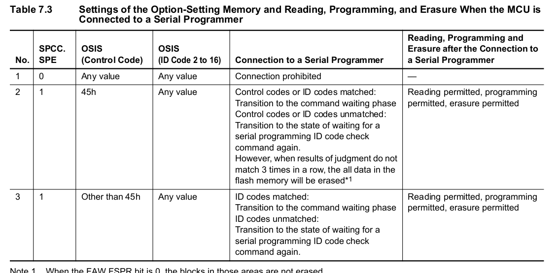
The connection can be totally prohibited, the number of ID code attempts can be unlimited or if do not match 3 times in a row, all the data in the flash memory can be erased.
This is not good. That means we can't use the serial interface to send more than 3 wrong ID codes. Maybe we could try to power off the device between tries... Let's take a look at the FINE interface:
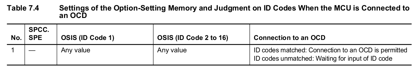
This is much better ! Using the FINE protocol we have an unlimited amount of tries. We could try to send read sequences with a bad ID and glitch the power to bypass the protection ! But wait, we don't know how FINE works :(
Reading the schematics and some datasheets tells us that FINE is a single wire interface. I can use the Renesas Flash Programmer (and control the communication speed) to get some activity on the bus and hook-up a scope and see what it looks like.
It seems to be some good old asynchronous serial communication. We can now connect an UART and log bytes. This is what it looks like:
8B 02 01 00 00 03 CD 01 FF FF FF FF C6 01 00 C6 01 00 C8 02 0B C6 01 00
Yeah, I know, there is one problem with half duplex communication: if you don't know the protocol, there is no way to detect who's talking. In order to discriminate the host and device in this communication I used this technique:
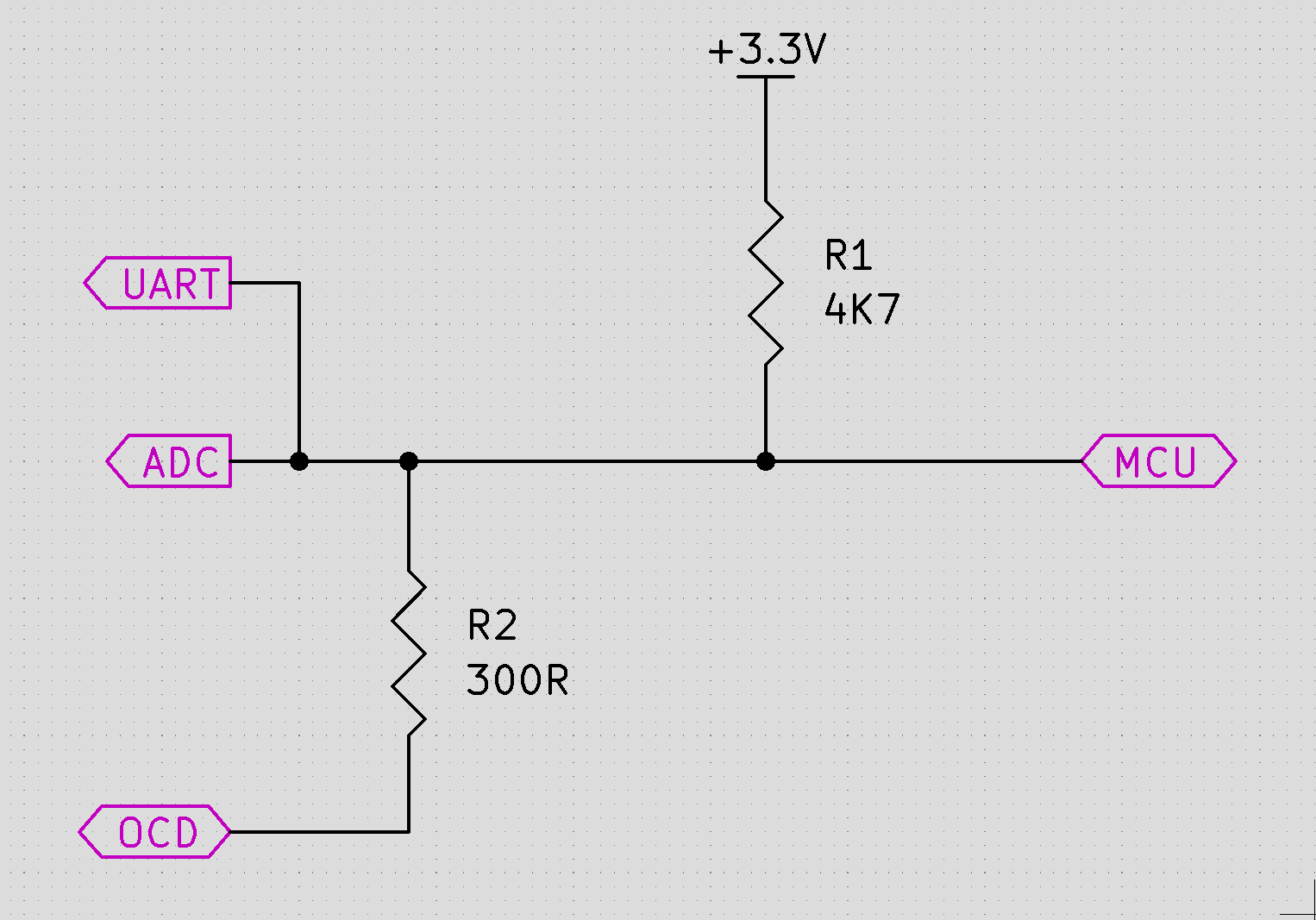
Normaly OCD and MCU would be connected directly. Here, I added a small resistor on the OCD side. We now have a divider. When MCU pulls the line low, the voltage at the center point (ADC) is 0V. However, when OCD pulls the line LOW there is a small voltage (about 200mV) at the center point. We now have a way to separate datas to and from our device.
So I used a NUCLEO board, wrote a program to listen to FINE and separate bytes depending on the voltage of '0' bits.
This is what it looks like:
H: 9D 43 75 C0
D: 23 02
H: 88 01 00 88 03 00 88 02 00 C6
D: 20 00
H: 84 55 00 00 00
D: 00
H: C4
The first thing I did when I started to work with this interface was to replay a capture I did while reading the configuration memory with the Renesas flash programmer. I did that for a while.
Then, a friend, who was also working on this with me, realized that the FINE protocol looked like the SCI protocol which is documented in the manual. SCI commands are just encapsulated inside FINE protocol. So let's quickly describe the SCI protocol.
The boot protocol is composed of COMMAND and STATUS packets:
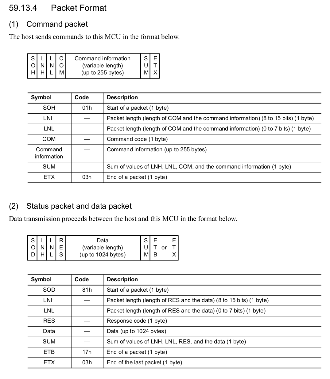
Though the sequence of transfer differs from command to command, common transfer sequences are used for the commands that only make settings for this MCU and for the commands that obtain information on the settings in this MCU:
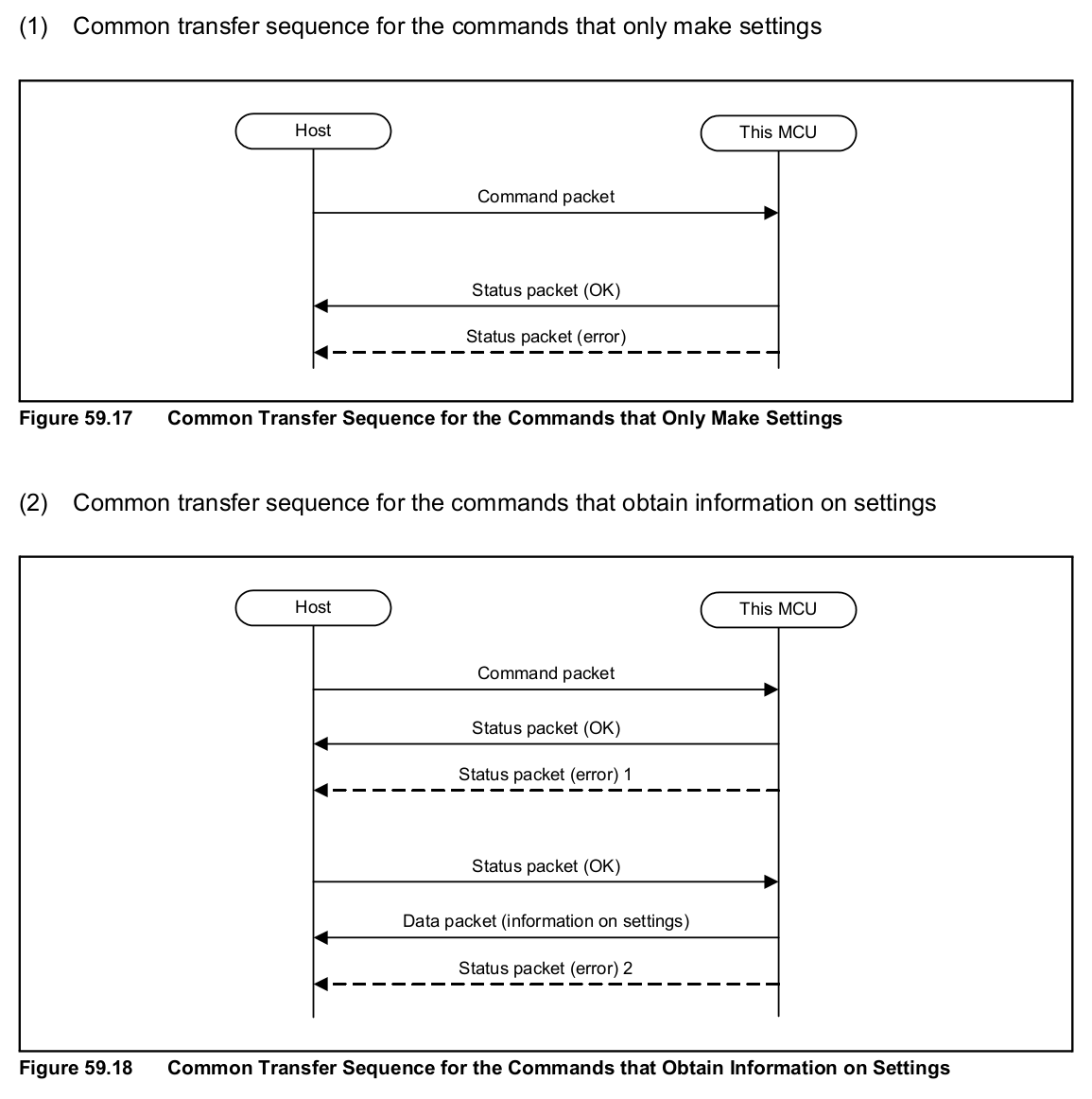
These figures are extracted from the User's Manual. For more information, please refer to it.
We now have enough information to start our comparison with FINE protocol.
Let's take an example:
H: 84 01 00 01 00
D: 00
H: C6
D: 00 00
H: 84 FF 03 00 00
D: 00

H: C4
D: 00 81 00 01 00
H: C4
D: 00 FF 03 00 00
H: C6
D: 00 00
Here you can see
01 00 01 00 FF 03
Which is (according to what we described in 5.2) a command packet (synchronization command):
01    -> Start of packet
00 01 -> Len
00    -> Command
FF    -> Sum
03    -> End of packet
and its status packet:
81 00 01 00 FF 03

81    -> Start of packet
00 01 -> Len
00    -> RES: (OK)
FF    -> Sum
03    -> End of packet
FINE frame length is limited to 5 bytes. Every chunk of data from one direction to the other will never be more than 5 bytes long.
HOST->MCU transfers always starts with 0x84. Then the MCU acks with a 0x00. HOST send 0xC6 (MCU ready ?) and MCU answers with a 0x00 0x00.
When HOST expects datas from MCU, it sends 0xC4. When it has enough datas, it sends 0xC6 and MCU responds with 0x00 0x00.
This is a very short description of the FINE protocol. This is not the subject here.
There is a lot more to do here. SCI only describes programming commands. I also logged traffic when the debugger was used and there is a lot more commands to understand (not documented this time) in order to reverse the debug protocol.
Now back to our main business.
The idea is to send a sequence to the MCU in order to read the flash section containing our legit ID code.
We are going to glitch the power supply of the MCU core just after the end of the "Serial Programming ID Code Check Command" (that's why understanding FINE can help).
As usual, when voltage glitching, we need to remove every capacitor on VCC and if possible find a direct connection to the Core power supply.
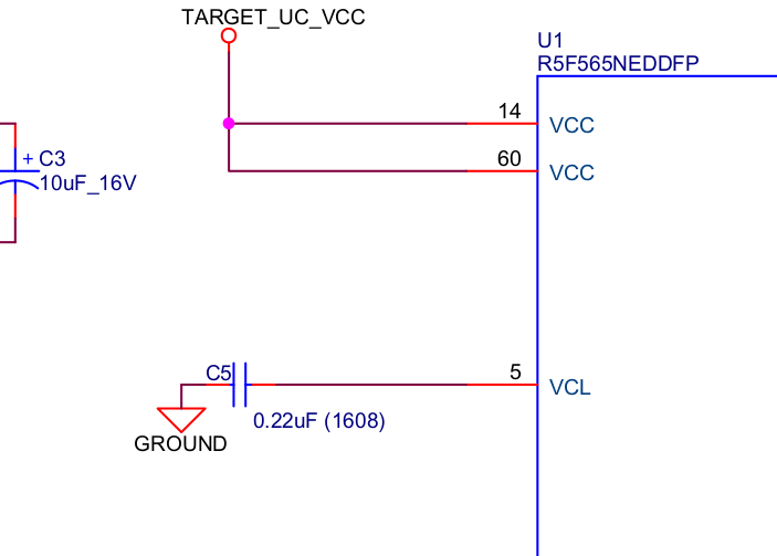
VCL is our target. In the User's Guide, one can read: "Connect to the VSS pin via a 0.22-μF multilayer ceramic capacitor for stabilizing the internal voltage."
This is where we're going to place our transistor.

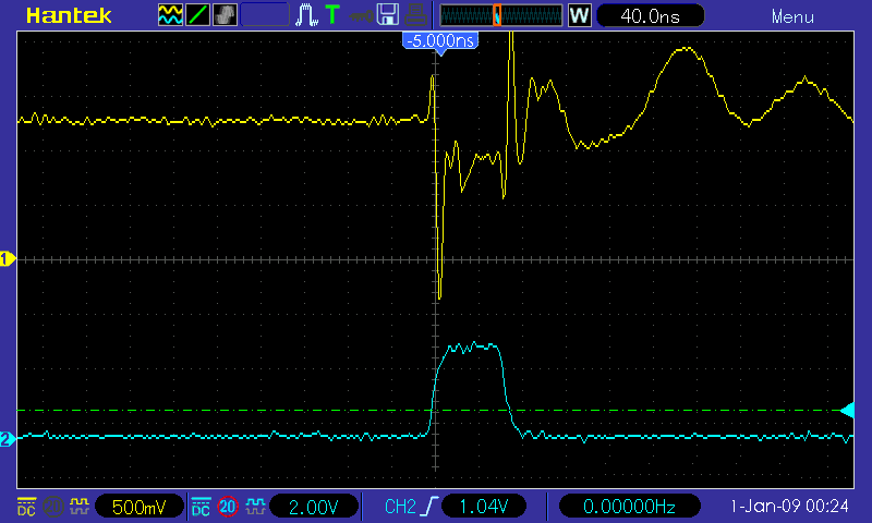
I used a NUCLEO-F429I board to implement the FINE protocol and produce the trigger for glitching.
The MCU and the internal timer used are running at 180MHz. This is pretty fast and can produce pulse width under 100ns:
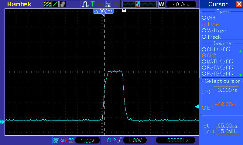
And this is the glitch observed at VCL pin:
The idea is simple:
After some time:
### RX65 FLASH EXTRACTOR ##

[*] Address 0xFE7F5D00
[*] Now trying trigger xxxxx

FE7F5D00: FF FF FF FF FF FF FF FF FF FF FF FF FF FF FF FF
FE7F5D10: FF FF FF FF FF FF FF FF FF FF FF FF FF FF FF FF
FE7F5D20: FF FF FF FF FF FF FF FF FF FF FF FF FF FF FF FF
FE7F5D30: FF FF FF FF FF FF FF FF FF FF FF FF FF FF FF FF
FE7F5D40: FF FF FF FF FF FF FF FF FF FF FF F8 FF FF FF FF
FE7F5D50: CC BB AA FF FF FF FF FF FF FF FF FF FF FF FF FF
FE7F5D60: FF FF FF FF FF FF FF FF FF FF FF FF FF FF FF FF
FE7F5D70: FF FF FF FF FF FF FF FF FF FF FF FF FF FF FF FF
We get the content of the option-setting memory !
Using the same method, I also tried to uncover "Reserved area" using the "Read Command". Normally, if you use this command to read addresses that you're not allowed to read, you get an error 0xD0 (address error).
Why not glitching it ? Of course it worked :)
I explored every "Reserved area" and all of them, excepted one returned only zeros and I eventually found the bootloader program.
Once we have a complete dump, we can use Ghidra and the RX extension thanks to ballon-rouge ( Here on github ). This extension targets RXv1 cores so few instructions are missing as our target is a RXv2 core.
We can confirm this is the bootloader and that we are glitching somewhere around this:
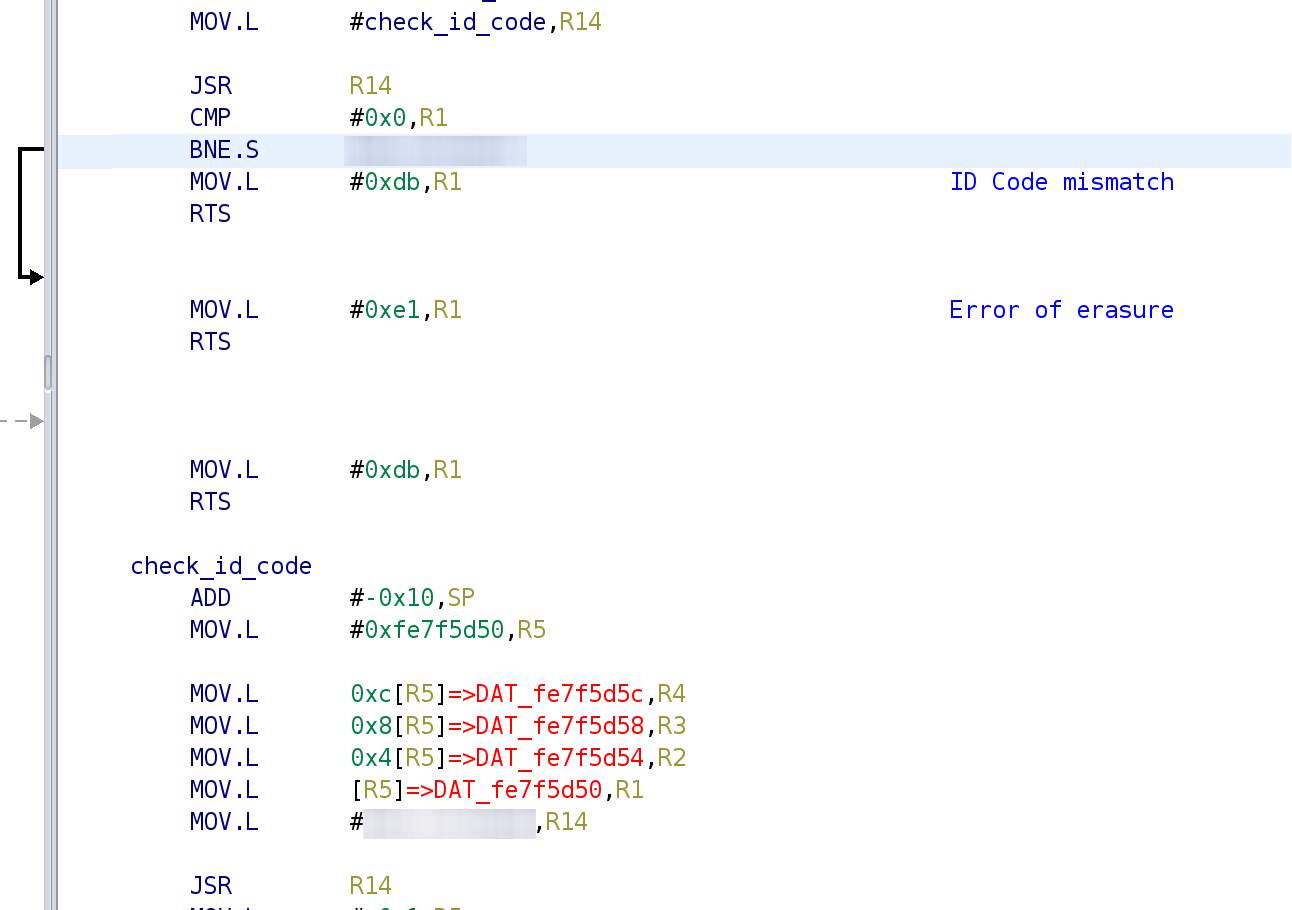
As you can see addresses 0xFE7F5D50 to 0xFE7F5D5F (which is the ID) are used.
This article proves one more time that power glitches are very powerful.
There is still some tasks I need to work on:
- complete disassembly of the bootloader,
- implementing the FINE programming protocol in OpenOCD,
- try to figure out how the debug protocol works.
Franck Jullien - 2021
Follow me on twitter! @fjullien06